


Exploring the Benefits of 850nm VCSEL in Sensing Applications
As a VCSEL manufacturer, we see every day how 850nm VCSEL technology has become a core building block for modern sensing systems. From consumer electronics to industrial automation and wearable health devices, this wavelength offers a very practical balance of eye safety, detector sensitivity and cost.
What Is an 850nm VCSEL?
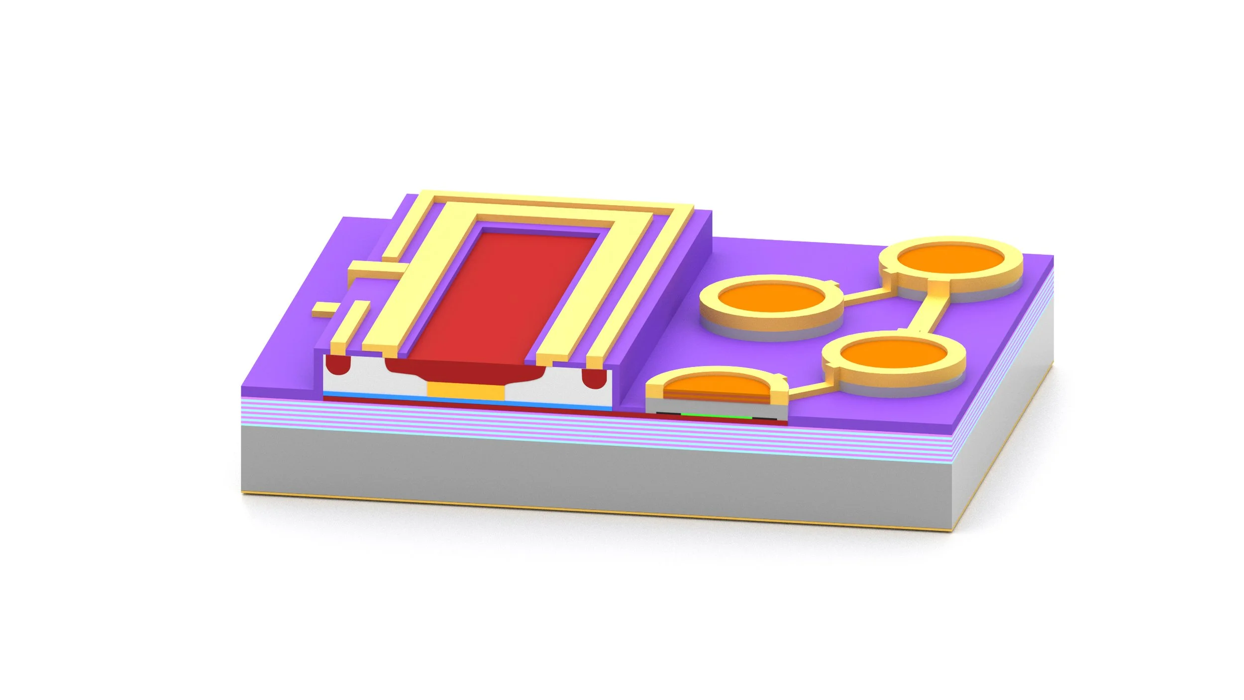
An 850nm VCSEL (Vertical-Cavity Surface-Emitting Laser) is a semiconductor laser that emits a narrow infrared beam vertically from the surface of the chip rather than from the edge. This vertical emission allows:
Wafer-level testing before dicing and packaging, improving yield and consistency.
Easy integration into arrays and compact modules, which is crucial for depth cameras, LiDAR and multi-channel sensors.
At Ace Photonics, we manufacture VCSEL laser diodes across key near-infrared bands, including 850 nm, specifically to match multimode fiber windows, eye-safety limits and optical sensor response curves.
Why 850nm VCSEL Stand Out in Sensing
1. Clean Signal and High Sensitivity
For many cameras and photodiodes, 850 nm sits in a very “comfortable” region of their spectral response. When you pair that with the narrow linewidth of a VCSEL, you get:
A high signal-to-noise ratio, especially when combined with IR bandpass filters on the receiver side.
Reduced background interference from ambient light compared with visible sources.
This directly translates into more reliable detection at lower optical power, which is essential in compact or battery-powered sensors.
2. Precision Beam and Accurate Measurements
Compared with broad-emitting IR LEDs, an 850nm VCSEL produces a stable, well-defined beam. For sensing this means:
Tight, near-circular spot profiles that simplify collimation and focusing.
Better control over divergence, so the illuminated region matches the intended field of view.
We supply both single-mode and multi-mode VCSELs, allowing system designers to trade off between beam quality and total output power depending on the sensing task.
3. Stable Wavelength and Long-Term Repeatability
Sensing algorithms are only as good as the stability of the light source. 850nm VCSELs offer:
Excellent wavelength stability over temperature, which is critical for systems that operate outdoors or in industrial environments.
Low drift over time, supporting long-term calibration and consistent factory testing.
Key Sensing Applications of 850nm VCSEL
As a manufacturer, we see 850nm VCSELs repeatedly specified in the following sensing scenarios:
3D depth and facial sensing: Dot-pattern or flood illumination for smartphone face unlock, AR/VR spatial mapping and gesture control.
Time-of-Flight (ToF) ranging: Distance measurement in consumer devices, industrial level sensing and robotic navigation.
Proximity and gesture sensing: Short-range detection in consumer electronics, gaming, smart home devices and human–machine interfaces.
Wearable and biomedical sensing: Heart-rate, SpO₂ and other biosensing functions where compact, low-power VCSELs can be integrated into watches and health bands.
Machine vision and industrial automation: Alignment, position sensing and part inspection where controlled IR illumination is preferred over visible light.
In many of these use cases, 850nm VCSEL arrays allow designers to distribute power across multiple emitters, improving redundancy and enabling flexible field-of-view control.
Custom 850nm VCSEL Options from Ace Photonics
Because sensing requirements are rarely identical from one project to another, we focus heavily on customization. For 850nm VCSELs we can support:
Output power levels: Typical options include 0.1 mW, 0.5 mW, 1 mW and 1.8 mW, allowing designers to match optical power to sensor distance, eye-safety class and power budgets.
Beam profile and divergence: Through cavity design, aperture geometry and front-end optics, we can tune from tight Gaussian spots to broader flood illumination, depending on whether you are building a ToF camera, LiDAR or simple proximity sensor.
Array geometry: 1D and 2D arrays with custom channel counts and pitch for structured light, multi-zone ranging or multi-point biosensing.
Modulation behavior: Optimization for high-speed digital modulation (e.g., ToF, coded illumination) or low-noise continuous-wave operation for analog sensing.
On the manufacturing side, our GaAs-based epitaxy and in-house chip processing (including ICP etching, wet oxidation and BCB processes) allow us to tailor device structures specifically for demanding sensing environments.
Flexible Packaging for Real-World Systems
The same 850nm VCSEL die can be adapted to different system architectures simply by choosing the right package. Ace Photonics provides:
TO-can packages for lab setups, instrumentation and robust industrial modules
Surface-mount (SMD / PLCC) packages for compact PCBs in high-volume devices such as wearables and consumer electronics
Custom and non-magnetic packages for specialized sensing tasks, including quantum and magnetic-field related applications at nearby wavelengths
These packages offer mechanical stability, thermal management and, where required, built-in optics to align the VCSEL output with the rest of the system.
Cost, Reliability and Lifetime Advantages
From a production viewpoint, 850nm VCSELs are designed to be both reliable and cost-effective:
Wafer-level testing reduces scrap and ensures only known-good die proceed to packaging.
The devices exhibit low power consumption and high efficiency, which lowers thermal stress and extends lifetime, especially in tightly packed sensors and modules.
Mature GaAs processing and standard surface-mount packages support high-volume, competitive pricing for consumer and industrial markets.
For customers, this means a sensing light source that not only meets technical specifications but also fits into real project budgets and product roadmaps.
850nm VCSELs vs Other Sensing Light Sources
When engineers evaluate light sources for sensing, the main alternatives to 850nm VCSELs are IR LEDs and edge-emitting lasers. From our experience:
Versus IR LEDs
VCSELs offer a narrower spectrum and more coherent beam, which improves signal clarity and depth accuracy.
They enable faster modulation, supporting ToF and advanced coding schemes that are difficult with broad-emitting LEDs.
Versus edge-emitting lasers (EELs)
Edge-emitting lasers can deliver higher power and longer range, but packaging and alignment are more complex and often more expensive.
VCSELs typically provide better cost per channel, simpler integration into arrays and easier thermal management—ideal for short- to mid-range sensing and dense multi-channel systems.
For most compact sensing modules, the combination of 850 nm wavelength, VCSEL architecture and tailored packaging gives an attractive balance of performance, safety, complexity and cost.
Conclusion
From our perspective as a VCSEL manufacturer, 850nm VCSELs have become a “go-to” choice for high-precision sensing. Their stable wavelength, controllable beam, efficient modulation and flexible packaging make them suitable for everything from consumer depth cameras to industrial automation and wearable biosensing.
By combining custom power levels (0.1–1.8 mW), array designs, package options and modulation behavior, Ace Photonics can align each 850nm VCSEL solution with the specific requirements of your sensing application—whether you are optimizing for accuracy, size, power budget or cost.