

Purpose-Built for Quantum technology
We develop precision VCSEL solutions for atomic clocks, quantum technology,
and advanced photonic systems for research, industrial, and emerging quantum applications.
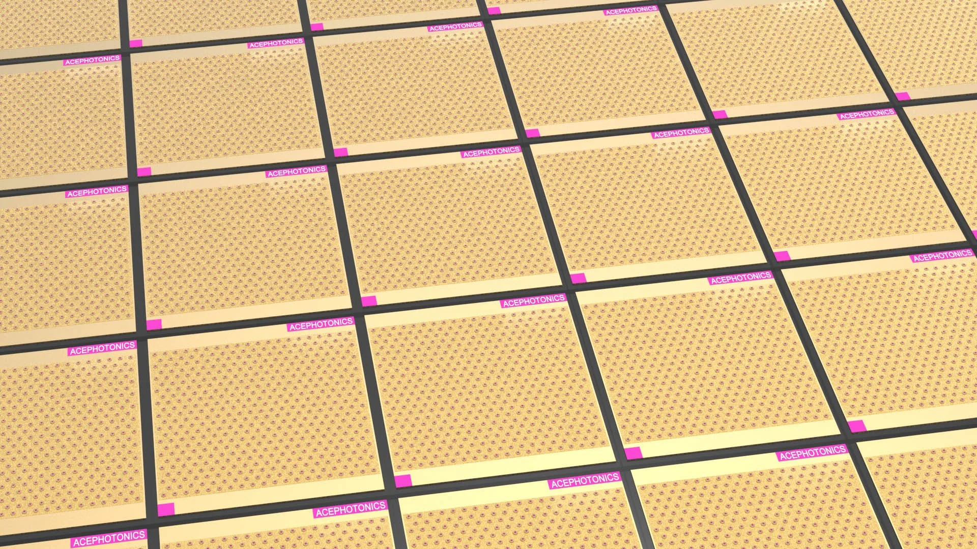
VCSEL Die
——Select VCSEL die by wavelength, output power, package type and application.
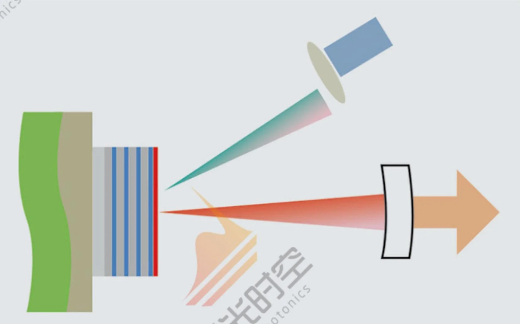
VCSELs are optoelectronic devices that combine the performance of traditional semiconductor lasers with the cost savings of LEDs. Unlike traditional edge-emitting lasers, VCSELs emit optical power from the surface of a wafer or chip. This enables wafer probing before chip sorting and packaging. In addition, VCSELs exhibit excellent wavelength stability over temperature and can be used with infrared bandpass filters to remove additional background noise from the received signal.
The high-power 795 nm/895nm 1 mW VCSEL developed by Ace Photonics Co., Ltd. is available in a variety of customizable packaging options (SMD, VCSEL TO46 packages, and VCSEL non-magnetic package ), making it suitable for diverse magnetometer designs. Our team has extensive experience collaborating with numerous research groups and industry partners both domestically and internationally.
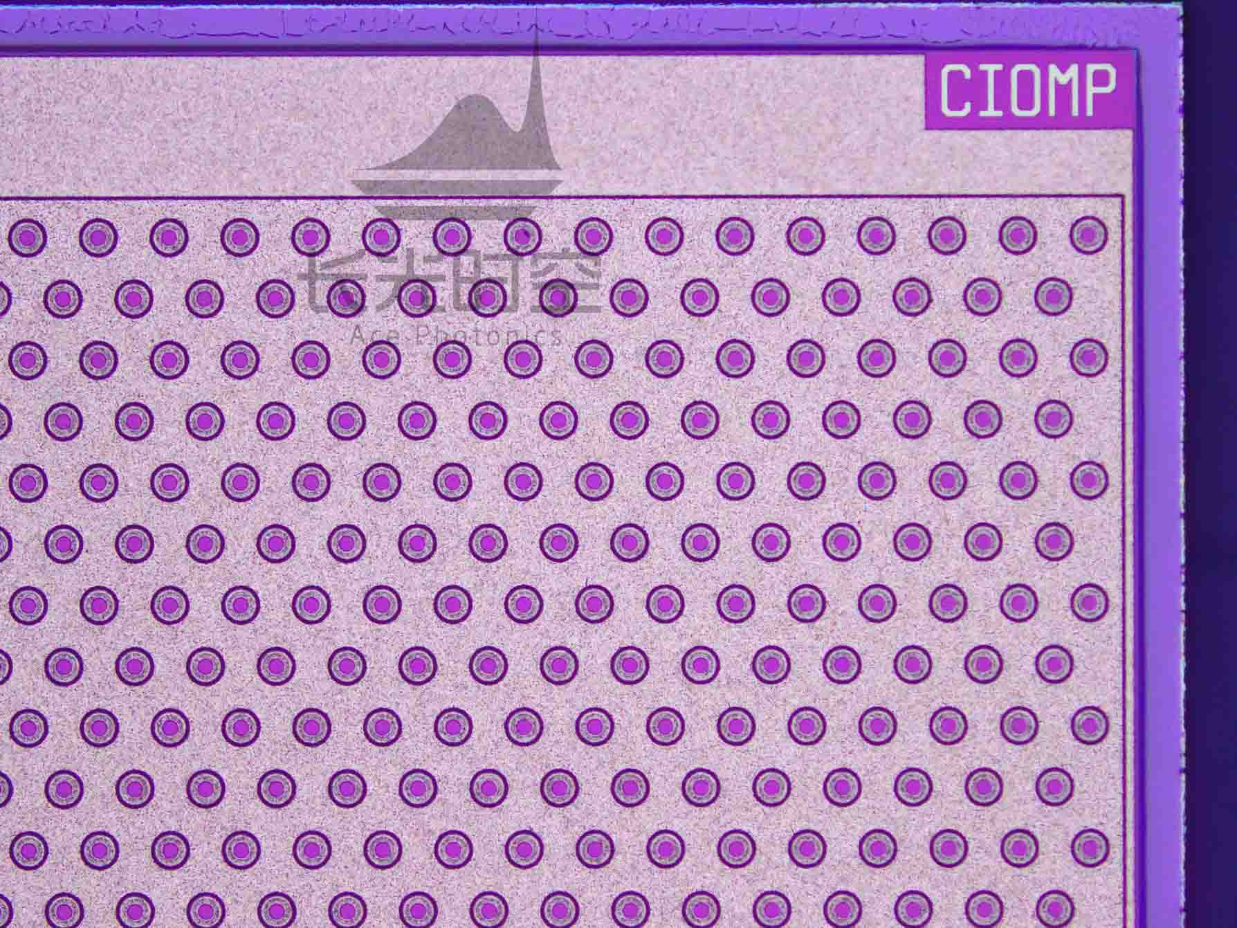
Die Drawings: Aperture Quantities
How to Choose a VCSEL Die
Core VCSEL Technologies in Our VCSEL Die:
Vertical resonant cavity structure
Current confinement technology
Thermal management technology
Polarization control technology
Wavelength control technology
Array and integration technology
Our VCSEL chip benefits from advanced semiconductor processing techniques that ensure optimal efficiency, reduced power consumption, and minimized heat generation. Our extensive range of bare die options is ideal for integration into various applications, including 3D sensing, facial recognition systems, LiDAR, optical communication networks, medical instrumentation, quantum sensing, and chip-scale quantum magnetometers.
Manufactured under stringent quality controls, our VCSEL die, SMD, VCSEL TO46 packages, and VCSEL non-magnetic package products provide unmatched flexibility, enabling seamless integration and customization within your product designs. Leveraging our cutting-edge wafer-level fabrication capabilities, each bare die undergoes rigorous testing and inspection, ensuring top-tier performance and durability.
VCSELs (vertical cavity surface emitting lasers VCSEL ) have various advantages over other types of lasers.
Include:
Surface emission, which offers design flexibility in addressable arrays
Low-temperature dependence of the lasing wavelength
Superior reliability
A wafer-level manufacturing process
These features make VCSELs better suited to various applications than conventional edge-emitting diode lasers and LEDs.
VCSEL technology includes epitaxial structure and chip design, epitaxial growth, front-end and back-end processing, packaging, and advanced testing and simulation. ACE PHOTONICS VCSELs are rated for operating ambient temperatures up to 150°C.

Ace Photonics VCSEL & Oxygen sensors
Wavelength-Specific Emission: VCSELs can be designed to emit light at wavelengths that are particularly suited for interaction with certain chemical substances, including oxygen-sensitive dyes.
High Modulation Speed: They can be modulated at high speeds, which allows for rapid and accurate measurements.
Temperature Stability: VCSELs provide stable output over various temperatures, which is crucial for precise measurements.
The combination of VCSEL technology with optical oxygen sensors results in highly effective and reliable tools for measuring oxygen concentration across various fields. The high efficiency, specific wavelength emission, and stability of VCSELs make them particularly well-suited for enhancing the performance of oxygen sensors. These VCSELs outperform edge-emitters in medical oxygen monitoring.
Ace Photonics VCSEL & 3D sensing
Today, facial recognition is 3D sensing’s primary application, but it is certainly not the only one. In the future, we see 3D sensing going much further and VCSEL is a vital component to enable it. Below are some of the key advantages of VCSEL in 3D Sensing applications.
Higher efficiency – VCSEL commonly achieves >45% at room temperature. The stacked material will have the ability of 6V per VCSEL.
Diffuser-less Illuminator – With the chip-level micro-optics array it will enable beam shaping. It also will help to reduce the chip cost by decreasing the packaging size.
Polarization – Demonstrated linear polarization chip for flood illuminator and structure light. narrow wavelength of +/-2nm over temperature. Improved SNR by a factor of four.
Low divergence – Typical VCSEL divergence >20o.but AMS can demonstrate a 10o low divergence chip with internal technology.
Ace Photonics' single-mode VCSELs have the advantages of a wide operating temperature range and high wavelength and polarization stability. According to the difference in power and operating temperature, our products are divided into intc0.1/1 mW and other series. The output power of our single-mode VCSEL is close to 5mW in the laboratory pre-development stage.
In addition, our single-mode VCSEL covers the 750-900nm band, improving energy efficiency while maintaining high output performance. Through integrated packaging, we integrate single-mode VCSEL chips with temperature controllers and temperature sensors to meet the requirements of various application environments.
Based on these advantages, we believe that single-mode VCSEL has become an ideal choice for atomic sensing spectroscopy, high-precision instruments, and other fields.
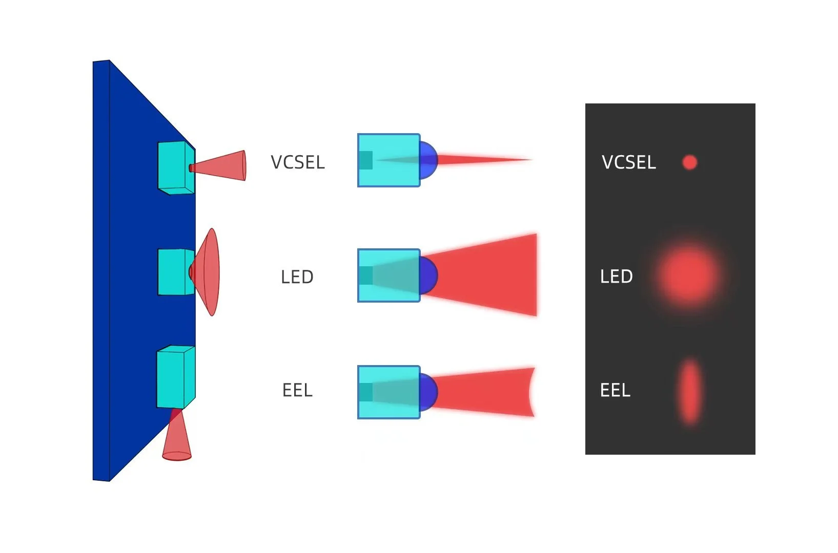
VCSELs possess performance advantages over both conventional LEDs and edge-emitting lasers.
Wafer Surface Emission
Surface emission allows full testing at the wafer level
High efficiency and low power consumption
Symmetric, low divergence output beams
Scalable die designs for high-power
Fast rise and fall times
Controllable single transversal mode and polarization
Exceptional wavelength stability with temperature
Flexibility in packaging
Ace Photonics VCSEL & Quantum Sensing
Vertical-Cavity Surface-Emitting Lasers (VCSELs) have become the light source of choice for modern quantum sensors. Their ultra-narrow linewidth, low threshold current, and superb beam quality let VCSELs efficiently pump or probe quantum media such as nitrogen-vacancy (NV) centers in diamond, alkali-vapor cells, and cold-atom ensembles.
Why Non-Magnetic Packaging VCSELs Matters
Quantum sensors detect minute magnetic, electric, or inertial signals; any ferromagnetic material in the opto-electronic package introduces stray fields that degrade accuracy. A non-magnetic VCSEL package—using ceramics, or specialty composites—keeps the magnetic background below the femtotesla level, preserves linewidth, and eliminates hysteresis drift during field sweeps. Commercial examples report order-of-magnitude improvements in signal-to-noise when substituting a non-magnetic VCSEL for a standard steel-can device.
Choose us
ACE PHOTONICSAdvantage 1
We have rich technical accumulation in the research and development of GaAs-based VCSEL lasers and can customize the epitaxial and device structure designs according to customer application requirements.
Advantage 2
We have rich experience in semiconductor laser chip processing, such as inductively coupled plasma etching(ICP), wet oxidation, and BCB processes.
Advantage 3
Relying on our experience in aerospace payload development and related testing conditions, customized product development can be carried out according to application in special environments.