


The Evolution of the VCSEL Diode: A Manufacturer’s Perspective
What Is a VCSEL Diode?
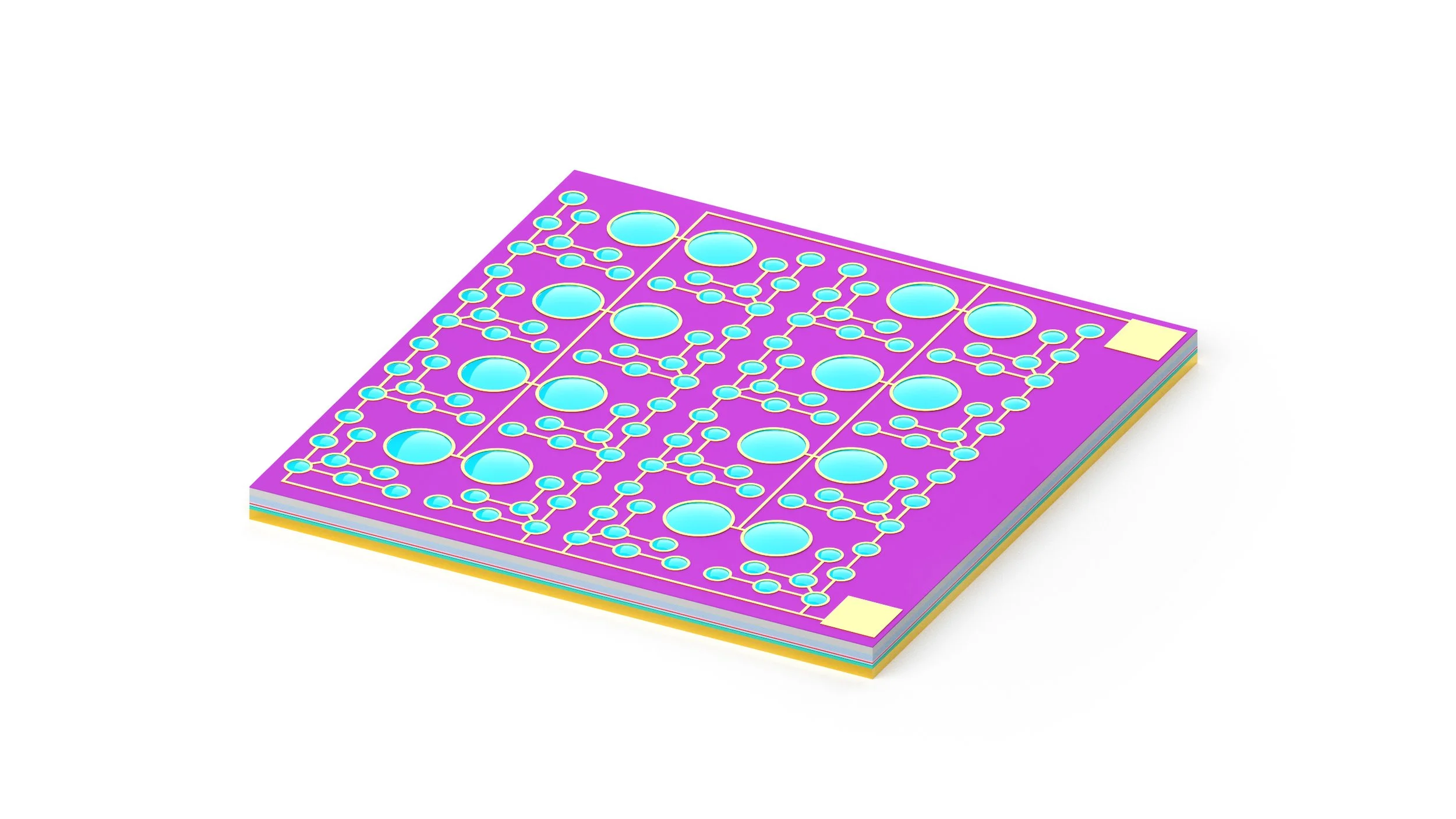
A VCSEL diode (Vertical-Cavity Surface-Emitting Laser) is a semiconductor laser that emits light perpendicular to the wafer surface. Two high-reflectivity distributed Bragg reflectors (DBRs) sandwich an active region, forming an ultra-short cavity.
Why that matters for real products
Low threshold, high efficiency. The short cavity reduces threshold current and supports dense arrays—ideal when every milliwatt counts.
Wafer-level testability. Vertical emission enables on-wafer probing before dicing, improving yield control and cost predictability.
Stable wavelength & clean beam. Useful for precision optical links and 3D sensing optics that require uniform illumination.
Packaging flexibility. From TO-packages to chip-on-submount (COS) with micro-lens arrays and diffractive optics.
As a manufacturer, we design VCSEL diodes to meet specific wavelength, far-field, modulation, and thermal targets—then verify performance at wafer and module level to lock in consistency over volume.
Why VCSEL Diodes Matter Now
Modern systems rely on the VCSEL diode for short-reach optical communications (intra-data-center and board-level links), 3D sensing (structured light, time-of-flight), barcode scanning, near-IR spectroscopy, and selected biomedical measurements. The device’s blend of efficiency, compact size, and fast modulation keeps it central as bandwidth and sensing demands rise.
Core application buckets
Data centers & enterprise I/O: multimode-fiber links, SR4/SR8 parallel optics, active optical cables.
Consumer & industrial 3D sensing: depth cameras, gesture/eye tracking, proximity sensing.
Measurement & healthcare: spectroscopy, flow cytometry illumination, pulse oximetry variants.
Logistics & retail: barcode and pattern-projected imaging.
From Lab Idea to Workhorse: Early Development & Hurdles
The VCSEL concept emerged in the 1970s. Practical engineering traction arrived in the late 1980s as epitaxy and microfabrication matured. Early prototypes faced low output power, mode control issues, reliability questions, and manufacturing cost. Progress in DBR reflectivity, oxide/implant confinement, thermal path design, and material quality gradually pushed VCSEL diodes to commercial readiness.
Technology Milestones That Unlocked Scale
Fabrication advances
MBE & MOCVD epitaxy: nanometer-level control over DBR stacks and quantum wells ensures tight wavelength bins and consistent thresholds.
Current & optical confinement: oxide apertures or ion implantation guide carriers and modes, lowering threshold and improving beam quality.
Array scaling & wafer-level test: standardized array architectures and automated assembly reduced cost per channel while boosting throughput.
Commercial adoption
Demand for high-speed, short-reach links in the 1990s accelerated VCSEL deployment in enterprise networks and data centers. As the tech matured, arrays spread into consumer 3D sensing and industrial metrology, where uniform, eye-safe illumination is critical.
Industry Impact & Where VCSEL Diodes Fit Best
1) Telecom & Data-Center Interconnects
VCSEL diodes excel in multimode-fiber environments: compact, low-power, and directly modulatable at multi-gigabit rates. Parallel arrays (e.g., SR4/SR8) compound total bandwidth while maintaining attractive energy per bit.
2) Enterprise & Personal Data Communication
From LANs to storage networks, VCSELs balance cost, power, and speed for short-distance Ethernet and high-throughput interfaces in servers, workstations, and peripherals.
3) Sensing & Imaging
Narrow linewidth and good tuning behavior suit structured-light and ToF depth sensing, near-range LiDAR, gesture recognition, and biomedical optics. VCSEL arrays pair well with diffractive optical elements (DOEs) to create precise, repeatable patterns.
Current Research & What’s Next
Active research themes
More optical power, higher wall-plug efficiency: better heat extraction, mode engineering, and reduced thermal resistance.
Wider wavelengths: pushing from visible to near-IR and SWIR to unlock new spectroscopy and sensing roles.
Higher symbol rates & deeper integration: co-design with drivers, co-packaged optics, and silicon photonics to lift bandwidth and cut system energy.
Emerging use cases
Robotics & ADAS: near-/mid-range perception and obstacle mapping.
AR/VR/MR: environment mapping, eye tracking, and hand/gesture tracking.
Next-gen compute fabrics: denser, lower-power optical I/O to relieve electrical bottlenecks.
How We Build Custom VCSEL Diode Solutions (Manufacturer’s Workflow)
1) Start with your system requirements
We work backward from your use case to define the device stack and layout:
Target wavelength & binning (e.g., 760–940 nm bands)
Beam characteristics (divergence, symmetry, M²)
Array geometry (pitch, emitter count, fill factor)
Modulation needs (OOK/PAM, rise/fall times)
Package & thermal path (COS, LGA, TO-can, heat spreaders)
Power budget & eye-safety envelope (IEC 60825-1-aligned design targets)
2) Engineer for your industry
Data-center optics: prioritize bandwidth per watt, temperature stability, and lifetime under elevated ambient conditions.
Sensing & biomedical: emphasize signal-to-noise, pattern quality with DOE integration, and eye safety.
Industrial & consumer: focus on shock/vibration robustness, EMI hygiene, and costed volume ramps.
3) Validate and qualify
Wafer-level screening for threshold, slope efficiency, wavelength, and near/far field.
Reliability testing across temperature/humidity, current stress, and optical power cycling.
Module-level verification with optics and drivers to prove system-level margins before scale-up.
FAQs About VCSEL Diodes (for search intent coverage)
Q1: What makes a VCSEL diode different from an edge-emitting laser?
VCSELs emit perpendicular to the wafer, enabling wafer-level testing, dense arrays, and easier packaging. Edge emitters typically offer higher single-emitter power but complicate array integration and test.
Q2: Are VCSEL diodes suitable for high-speed links?
Yes. VCSELs support direct modulation at multi-Gb/s and scale via parallel arrays for very high aggregate bandwidth over multimode fiber.
Q3: How do you ensure wavelength stability in mass production?
Through tight epitaxy control (DBR and quantum wells), temperature management, and binning based on wafer-level test results.
Q4: Can VCSEL arrays be shaped for 3D sensing patterns?
Absolutely. Arrays integrate with diffractive optical elements or micro-lens arrays to produce tailored dot fields or illumination profiles.
Q5: How do you balance eye safety with output power?
We design to the target class limits and tune aperture sizes, pulse width, duty cycle, and optical train to stay within safety margins while meeting SNR.