
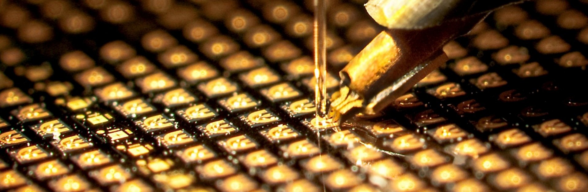
VCSEL Manufacturers for Custom Dies, Packages and Modules
Choosing between VCSEL manufacturers requires more than comparing a nominal wavelength and maximum output power.
The selected manufacturer must be able to connect the semiconductor design, chip-processing method, optical performance, package structure, thermal behavior and production testing with the requirements of the final system.
This is particularly important for applications such as atomic sensing, spectroscopy, 3D sensing and precision instrumentation. In these systems, a small difference in wavelength, optical mode, polarization, package material or temperature response can affect whether the VCSEL operates correctly after integration.
Ace Photonics develops VCSEL dies, packaged devices, gain chips and application-specific modules. Available options include standard and custom wavelengths, TO-can and SMD packages, non-magnetic package structures and OEM development support.
What Should Buyers Expect from VCSEL Manufacturers?
A VCSEL manufacturer should do more than supply a laser chip.
Depending on the project, the manufacturer may need to support:
Semiconductor and vertical-cavity design
Wavelength and output-power selection
Single-mode or multimode operation
VCSEL die processing
Wafer-level electrical and optical testing
TO-can, SMD or ceramic packaging
Non-magnetic material selection
Thermal management
Window, coating and lens integration
Thermistor or TEC integration
Prototype development
Production testing and performance binning

Not every manufacturer provides all these capabilities internally. Some companies focus on standard catalog products, while others support application-specific device, package or module development.
Before selecting a supplier, customers should determine which part of the development process they need the manufacturer to manage.
Why VCSEL Manufacturing Requires Specialized Control
A VCSEL, or Vertical-Cavity Surface-Emitting Laser, emits light perpendicular to the surface of the semiconductor wafer.
Its active region is positioned between two distributed Bragg reflector mirrors. These DBRs form the short vertical optical cavity that controls resonance and contributes to the final emission wavelength.
VCSEL manufacturing combines several closely connected processes:
Epitaxial structure design and growth
Lithography and mesa formation
Etching
Current-confinement formation
Metallization
Passivation and planarization
Wafer-level testing
Die separation
Die attachment and wire bonding
Package assembly and final testing
Variation at any stage can affect wavelength, threshold current, output power, beam profile, optical mode or reliability.
For example, epitaxial layer thickness influences cavity resonance and DBR reflectivity. Oxidation control influences aperture diameter and current confinement. Package assembly affects heat transfer, mechanical stress and optical alignment.
VCSEL manufacturers should therefore control both the chip and the conditions in which the chip will operate.
Ace Photonics as a VCSEL Manufacturer
Ace Photonics was established in Wuxi, China, in 2022. Its current company profile states that its technical team has more than 20 years of semiconductor-laser experience and that the company supports GaAs-based VCSEL structure design, ICP etching, wet oxidation and BCB processing.
The company also lists ISO 9001:2015 certification, intellectual-property-management certification and more than 15 authorized invention patents.
Ace Photonics focuses on four main product levels:
This product structure allows customers to select the integration level that matches their own design and manufacturing capabilities.
VCSEL Die Options
A bare VCSEL die provides the greatest freedom for customers that already have chip-bonding, packaging or module-integration capabilities.
VCSEL dies may be selected according to:
Target wavelength
Output power
Emitting-aperture size
Single-mode or multimode operation
Beam divergence
Spectral behavior
Polarization
Operating temperature
Die dimensions
Bond-pad layout
Testing and binning requirements
Ace Photonics currently lists VCSEL die options around:
760 nm
790/795 nm
850 nm
880 nm
890/895 nm
Its published product table also includes multiple output-power options and bare-die, TO, customized and non-magnetic package configurations. Final availability and performance should be confirmed against the relevant product datasheet and operating conditions.
Learn more about available VCSEL die options.
Single-Mode and Multimode VCSEL Manufacturing
One of the first decisions when working with VCSEL manufacturers is whether the application requires single-mode or multimode output.
Single-Mode VCSELs
Single-mode VCSELs are commonly evaluated for applications that require controlled optical behavior, such as:
Atomic sensing
Atomic clocks
Spectroscopy
Precision measurement
Optical reference systems
Application-specific fiber or free-space coupling
Important single-mode parameters may include:
Center wavelength
Wavelength tolerance
Spectral width
Side-mode behavior
Polarization
Beam divergence
Output power
Temperature tuning
Current tuning
Mode stability across the operating range
Single-mode performance should not be evaluated at only one current and room temperature. Customers should define the complete current and temperature range over which the required optical mode must be maintained.
Multimode VCSELs
Multimode VCSELs are often selected when total output power, illumination area or array integration is more important than maintaining a single transverse mode.
Applications may include:
3D sensing
Time-of-flight sensing
Proximity sensing
Illumination
Industrial sensing
Short-reach optical communication
VCSEL arrays
When evaluating multimode devices, customers may need to confirm far-field distribution, power uniformity, array configuration, pulse conditions and thermal roll-over.
VCSEL Wavelength Selection
The correct wavelength depends on the target material, detector response, optical filter, atomic transition and environmental conditions of the system.
A nominal wavelength alone is not enough. VCSEL manufacturers and customers should also confirm:
Center-wavelength tolerance
Wavelength at the intended operating current
Wavelength at minimum and maximum temperature
Current-tuning coefficient
Temperature-tuning coefficient
Spectral width
Side modes
Required tuning range
Batch-to-batch tolerance
For example, systems based on rubidium atomic transitions may evaluate VCSELs around 795 nm, while cesium-based systems may require devices around 895 nm.
General sensing and communication systems may instead use wavelengths such as 760 nm, 850 nm or 880 nm, depending on the detector, optical path and measurement method.
See the VCSEL wavelength and product selection guide for additional selection information.
VCSEL Package Options
The package protects the VCSEL die and provides the mechanical, electrical, thermal and optical interface between the chip and the final system.
Package choice can affect:
Device dimensions
Mounting method
Heat dissipation
Optical alignment
Window transmission
Back reflection
Electrical parasitics
Environmental protection
Magnetic compatibility
Production assembly
Ace Photonics currently presents TO-can, SMD, ceramic, non-magnetic and custom package options. Its OEM service also lists optional TECs, temperature sensors, windows, lenses, beam shaping, driver integration and PCB or module development.
TO-Can VCSEL Package
A TO-can package can be appropriate for:
Laboratory evaluation
Engineering prototypes
Optical instruments
Industrial sensing
Systems requiring easy handling
Applications requiring a window or lens
Before selecting a TO-can package, customers should confirm package dimensions, pin layout, window material, thermal path and whether conventional metal components are acceptable.
SMD VCSEL Package
An SMD package can support:
Compact PCB integration
Automated assembly
Wearable or portable devices
3D sensing systems
Proximity sensors
Higher-volume production
Important considerations include reflow temperature, PCB layout, optical-axis position, package coplanarity and thermal resistance.
Non-Magnetic VCSEL Package
A non-magnetic package may be required when the VCSEL operates near a magnetically sensitive sensor.
Typical applications include:
Atomic magnetometers
Quantum sensors
Atomic clocks
Precision magnetic measurement
Magnetically sensitive laboratory instruments
The package housing is only one possible source of magnetic interference. Pins, plating, bonding materials, solder, adhesives, thermistors, TECs and surrounding electronics may also need to be evaluated.
Customers should define material restrictions and system-level magnetic requirements before package development begins.
Learn more about non-magnetic VCSEL packaging.
Custom VCSEL Package
A custom package may be needed when standard TO-can or SMD formats cannot meet the project requirements.
Customization may include:
Housing dimensions
Pin configuration
Mounting reference
Optical aperture
Window material
Anti-reflection coating
Lens integration
Beam shaping
Thermistor integration
TEC integration
Non-magnetic materials
Driver and PCB integration
Application-specific module assembly
Custom development should begin with measurable requirements rather than only a general application description.
VCSEL Manufacturing Processes
When comparing VCSEL manufacturers, buyers should ask which semiconductor and assembly processes are available and how those processes are controlled.
A list of processes is not enough by itself. Customers should also ask how the manufacturer monitors variation and how the final products are tested against the agreed specification.
Wafer-Level and Final VCSEL Testing
The surface-emitting structure of a VCSEL allows electrical and optical measurements while the devices are still on the wafer.
Depending on the project, wafer-level testing may include:
Threshold-current measurement
Operating-voltage measurement
Output-power measurement
Center-wavelength measurement
Spectral screening
Leakage-current testing
Wafer mapping
Performance binning
After packaging, additional testing may be required because die attachment, wire bonding, thermal resistance, windows and optical components can change the operating conditions.
Final tests may include:
L-I-V characterization
Optical spectrum
Beam divergence
Far-field distribution
Polarization
Temperature-dependent wavelength
Temperature-dependent power
Modulation response
Package inspection
Reliability testing
The testing plan should reflect the intended application. A VCSEL for laboratory evaluation may not need the same qualification process as a component intended for volume production or a special operating environment.
Custom VCSEL Development Process
A clear development process helps reduce misunderstanding between the customer and manufacturer.
A typical custom VCSEL project may follow these stages:
1. Requirement Review
The customer provides the application, target wavelength, output power, optical mode, temperature range, package type and expected quantity.
The manufacturer reviews whether an existing product can meet the requirement or whether customization is needed.
2. Product or Structure Selection
The project may begin with:
An existing VCSEL die
A modified die configuration
A custom package
A custom optical interface
A new module design
A more extensive device-development project
Using an existing qualified die can reduce development risk when only the package or optical interface needs to change.
3. Optical and Mechanical Design
The manufacturer and customer confirm:
Package dimensions
Pin configuration
Die position
Optical axis
Window or lens
Thermal path
Mounting method
Material requirements
4. Engineering Samples
Samples are produced so the customer can evaluate the VCSEL in the actual system.
The evaluation should use representative current, temperature, optical and mechanical conditions.
5. Testing and Design Review
Test results are compared with the agreed requirements. If necessary, the package, operating condition or device selection is adjusted.
6. Production Preparation
Before volume production, both parties should agree on:
Final specification
Test conditions
Acceptance limits
Sample approval
Documentation
Packaging and shipping method
Production quantity
Change-control process
Ace Photonics describes its OEM workflow as requirement discussion, optical and mechanical design, testing, sample development and volume production.
Applications Supported by VCSEL Manufacturers
A manufacturer may serve many industries, but customers should evaluate whether it has relevant experience with the specific requirements of their system.
Quantum and Atomic Sensing
Quantum and atomic systems may require:
795 nm or 895 nm wavelength options
Single-mode output
Controlled polarization
Temperature tuning
Compact packaging
Non-magnetic materials
Thermistor or TEC integration
The manufacturer should understand that package materials and nearby electrical components can affect the complete sensing environment.
Spectroscopy and Gas Sensing
Spectroscopy and gas-sensing applications may require:
Target absorption wavelength
Narrow spectral output
Current or temperature tuning
Stable optical power
Appropriate window and coating
Detector and filter compatibility
The wavelength requirement should be defined according to the target medium and optical system.
3D and Proximity Sensing
3D sensing systems may prioritize:
Optical output power
Pulse operation
Array configuration
Beam distribution
Compact SMD packaging
Micro-optics integration
Thermal management
Production repeatability
Laser-safety evaluation remains a system-level responsibility and must consider the driver, optics, pulse conditions and final enclosure.
Industrial and Precision Measurement
Industrial systems may require:
Wide operating-temperature range
Mechanical stability
Consistent wavelength and power
Robust packaging
Environmental protection
Traceable testing
Long-term product availability
The manufacturer should evaluate the actual environment rather than assuming that all industrial applications have the same requirements.
How to Compare VCSEL Manufacturers
The following table can be used when evaluating potential suppliers.
The best VCSEL manufacturer is not necessarily the company with the longest product list. It is the supplier whose verified capabilities match the requirements and development stage of the project.
Information to Provide When Contacting VCSEL Manufacturers
Clear requirements allow the manufacturer to evaluate feasibility and recommend the correct product more efficiently.
Drawings, optical layouts and interface documents should also be provided when the VCSEL must fit an existing system.
Why Work with Ace Photonics?
Ace Photonics focuses on VCSEL products for sensing, atomic systems, industrial applications and specialized photonic integration.
Available support may include:
GaAs-based VCSEL structure evaluation
Standard and custom wavelengths
Single-mode and multimode products
VCSEL dies
TO-can and SMD packages
Non-magnetic packages
Custom windows and lenses
Thermistor and TEC integration
VCSEL gain chips
Application-specific modules
Engineering samples
OEM package development
Rather than selecting a product from the nominal wavelength alone, customers can provide the complete optical, electrical, thermal and mechanical requirements for technical review.
Frequently Asked Questions
What do VCSEL manufacturers produce?
VCSEL manufacturers may produce bare dies, packaged VCSELs, arrays, gain chips and integrated modules. The available product level depends on the supplier’s semiconductor, packaging and optical-integration capabilities.
What is the difference between a VCSEL manufacturer and a VCSEL supplier?
A manufacturer participates directly in the design, processing, testing or packaging of the VCSEL. A supplier may distribute products manufactured by another company. Some businesses perform both roles.
Can VCSEL manufacturers provide custom wavelengths?
Some manufacturers can adjust the epitaxial structure or select existing designs to meet a target wavelength. Feasibility depends on the wavelength, tolerance, power, quantity and development scope.
Can the same VCSEL die use different packages?
Yes. A compatible die may be assembled in TO-can, SMD, ceramic, non-magnetic or custom packages. The final package must still meet the thermal, electrical, optical and mechanical requirements of the device.
What is a non-magnetic VCSEL package?
A non-magnetic VCSEL package uses selected materials and structures intended to reduce magnetic interference near sensitive instruments. The complete package and surrounding system should be evaluated against the project’s magnetic requirements.
How should I evaluate a VCSEL sample?
Test the sample under representative current, temperature, modulation, optical and mechanical conditions. Confirm wavelength, output power, optical mode, beam profile and package compatibility across the intended operating range.
What information is needed for a custom VCSEL project?
Provide the application, wavelength, power, optical mode, temperature, package, electrical conditions, optical interface, quantity, testing requirements and project schedule.
Can Ace Photonics support both samples and production?
Ace Photonics provides engineering-sample and OEM development services. Production feasibility, sample quantity and delivery terms should be confirmed for the selected product and configuration.
Request VCSEL Product Information
When contacting Ace Photonics, send your application, target wavelength, output power, package preference, operating temperature and required quantity.
The engineering team can evaluate whether an existing VCSEL die, packaged product, gain chip or custom module is the most suitable starting point.
Contact Ace Photonics to request datasheets, engineering samples or a custom VCSEL evaluation.