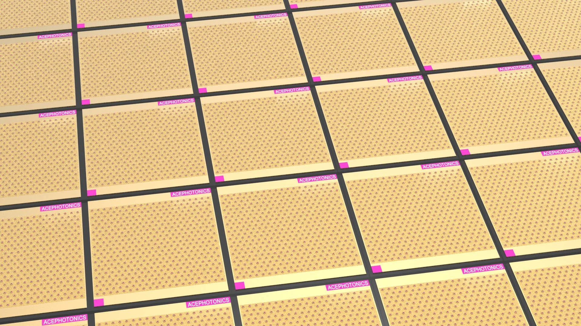
Boost System Efficiency with High-Performance VCSEL Chip (Die)
When you’re building a fast optical link, a reliable depth-sensing module, or a precision instrument that can’t drift, the light source is not a “small part.” It’s the performance anchor. A VCSEL chip (die) gives you that anchor in a compact footprint—plus the manufacturing advantages that make scale-up realistic.
At Ace Photonics, we manufacture GaAs-based VCSEL die and support multiple integration levels (bare die, packaged devices, and arrays). The goal is simple: help you ship products that hit spec, stay stable over temperature, and keep power budgets under control.
What Is a VCSEL Chip (Die)?
A VCSEL (Vertical-Cavity Surface-Emitting Laser) emits light vertically from the wafer surface rather than from a cleaved edge. That structure matters because it enables:
Wafer-level testing before dicing and packaging
Tight binning for consistent performance in volume
Easy scaling from single emitters to dense 1D/2D arrays
Compact optical engines for both datacom and sensing
In other words: VCSEL architecture isn’t just “different.” It’s engineered for repeatability.
Why VCSEL Die Improves Throughput per Watt
Efficiency is not only about saving energy—it’s about getting cleaner signals, simpler thermal design, and better end-user performance. Our VCSEL chip platforms are designed around practical system targets:
1) Lower power and reduced thermal load
High electrical-to-optical efficiency helps you reduce heat generation, which can simplify heatsinking and improve long-term stability—especially in dense optical modules.
2) Beam shape that’s easier to couple
The near-circular output typical of VCSELs makes coupling and alignment more forgiving in many optical assemblies.
3) Stable wavelength behavior
For sensing (and many filtered optical systems), wavelength control improves signal quality and measurement robustness across temperature changes.
Applications: Where VCSEL Chip (Die) Delivers the Most Value
A single VCSEL technology base can support both high-speed links and high-precision measurements—useful when your product portfolio spans more than one market.
Optical communications & datacom
Short-reach optical links, active optical cables, optical transceivers
High-density port architectures enabled by compact form factor and array potential
Cleaner modulation behavior for stable link performance
3D sensing, imaging, and LiDAR
Structured-light projection and time-of-flight (ToF) illumination
Depth mapping, facial recognition, gesture detection
Options for array layouts optimized for micro-optics or diffractive elements
Medical & wearable sensing
Optical sensing stacks for physiological monitoring (e.g., SpO₂ / tissue oxygen)
Narrowband emission can improve signal integrity under motion and across environments
Gas & environmental sensing
Narrowband IR light sources suitable for optical sensing methods that rely on spectral selectivity
Quantum & atomic sensing
VCSELs tuned to specific absorption lines (common around rubidium/cesium transitions)
Packaging options that support noise-sensitive instruments, including non-magnetic builds when required by the system environment
What We Control at the Wafer Level (So You Don’t Fight Variability Later)
A VCSEL die is only as good as its control plan. Our process emphasizes wafer-level characterization so performance is managed early, not “fixed” in final assembly.
Key parameters we typically control and bin at wafer level include:
Threshold current
Output power
Wavelength spread / wavelength stability
Beam profile / divergence targets
Mode and polarization consistency (design-dependent)
LIV and spectral mapping results for early binning before singulation
From Design to Fabrication: What’s Inside Our VCSEL Manufacturing Flow
We keep critical VCSEL steps linked in a single process flow to reduce lot-to-lot variability and shorten iteration cycles:
GaAs MOCVD/MBE epitaxy with engineered DBR mirror stacks
Mesa patterning and ion implantation
Selective oxidation for stable oxide apertures
Front-/back-end metallization tailored to your assembly approach (wire-bond or flip-chip)
For new programs, we also support structured design-of-experiments (DOE) lots—helpful when you’re dialing in aperture, cavity, or thermal paths to meet a tight operating window.
Typical VCSEL Die Options (Examples)
Depending on your use case, you may start from bare die and build your own optics, or you may prefer a package that drops into your line. We support both approaches.
Common wavelength families used in sensing and precision instrumentation (including variants around 760/763 nm, 790/795 nm, and 890/895 nm)
Typical output-power classes offered across multiple options (for example, 0.1 mW / 1 mW / 1.8 mW categories in specific product families)
Packaging options such as SMD, TO-can (e.g., TO46), and non-magnetic packages
Designs intended for wide operating temperature use cases (including solutions rated for high-temperature environments up to 150°C in applicable platforms)
If you need die drawings (e.g., aperture quantities) or datasheets, we can provide the matching documentation set for the configuration you’re targeting.
How to Get Started (Fast, Without Over-Spec’ing)
To recommend the right VCSEL chip (die), we usually align on a few practical inputs:
Target wavelength and acceptable wavelength drift vs. temperature
Required optical power at operating temperature (CW or pulsed)
Beam/divergence and illumination pattern needs (single emitter vs. array)
Electrical constraints (driver, bias, modulation)
Packaging/assembly plan (wire-bond, flip-chip, SMT) and reliability goals
Once those are clear, we can propose a die/platform option and a binning/test plan that matches how you build products in the real world.


