Purpose-Built for Quantum technology
We develop precision VCSEL solutions for atomic clocks, quantum technology,
and advanced photonic systems for research, industrial, and emerging quantum applications.
Understanding VCSEL L-I-V Curves: Threshold Current and Optical Power
When evaluating a Vertical-Cavity Surface-Emitting Laser (VCSEL), the most critical diagnostic tool at your disposal is the VCSEL L-I-V curve. This single plot integrates optical output power (L), drive current (I), and forward voltage (V) onto a unified coordinate system, providing a direct view of device efficiency, series resistance, and thermal performance.
Below is an engineering analysis of how to read these curves, calculate key operating parameters, and select optimal packaging for precision applications.
The Core Parameters of the L-I-V Plot
A standard VCSEL characterization setup sweeps the injection current while monitoring both the optical flux emitted from the top surface and the resulting voltage drop across the diode junction.
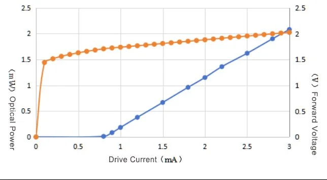
Referencing the test data shown in the figure above:
| Drive Current (I) | Optical Power (L) | Forward Voltage (V) | Operating State |
|---|---|---|---|
| 0.0 mA to 0.7 mA | ≈ 0 mW | 0.0 V → 1.68 V | Sub-threshold spontaneous emission (LED mode) |
| 0.8 mA | ≈ 0.02 mW | ≈ 1.71 V | Threshold Point (Ith); lasing turn-on |
| 1.0 mA | 0.20 mW | 1.75 V | Linear lasing regime |
| 1.5 mA | 0.68 mW | 1.82 V | Linear lasing regime |
| 2.0 mA | 1.15 mW | 1.89 V | Linear lasing regime |
| 2.5 mA | 1.62 mW | 1.97 V | Linear lasing regime |
| 3.0 mA | 2.10 mW | 2.05 V | High-efficiency linear output |
1. Optical Power (L, Blue Line)
Below 0.8 mA, the blue line sits flat against the horizontal axis. In this region, carrier recombination inside the quantum wells is purely spontaneous, producing weak, incoherent light.
Once current crosses the 0.8 mA knee, optical gain matches internal microcavity and mirror losses. Stimulated emission takes over, carrier density clamps at threshold, and coherent output power scales linearly with injection current.
2. Forward Voltage (V, Orange Line)
The orange curve displays two distinct slope regions:
- Bandgap Turn-On (0 to 0.2 mA): Voltage ramps sharply up to approximately 1.5 V as bias overcomes the p-n junction barrier.
- Ohmic Series Resistance (>0.5 mA): The voltage curve transitions into a gentle linear incline, rising from 1.7 V to 2.05 V at 3.0 mA. The slope of this line reflects the series resistance (Rs) introduced primarily by the alternating hetero-interfaces within the p-doped and n-doped Distributed Bragg Reflector (DBR) stacks.
Key Metrics Extracted from the L-I-V Curve
Threshold Current (Ith)
Threshold current marks the minimum current needed to initiate lasing. On automated test benches, it is calculated using:
- Linear Extrapolation: Fitting a line through the linear portion of the power curve and finding its intersection with the L = 0 axis. For this device, that intercept falls directly at 0.8 mA.
- Second Derivative (d²L/dI²): Locating the maximum peak of the second derivative, pinpointing the inflection where the curve transitions from spontaneous to stimulated emission.
Slope Efficiency (ηs)
Slope efficiency measures how effectively current injected above threshold converts into optical power:
Using points from the linear section:
- At I1 = 1.0 mA, L1 = 0.20 mW
- At I2 = 3.0 mA, L2 = 2.10 mW
A slope efficiency of 0.95 W/A indicates strong internal quantum efficiency and minimal parasitic leakage around the oxide aperture.
Differential Series Resistance (Rs)
Series resistance dictates heat generation via Joule heating (I²Rs). It is extracted from the voltage slope past turn-on:
Thermal Rollover Considerations
While the plotted device displays linear output up to 3.0 mA (2.1 mW), pushing drive current significantly higher eventually leads to thermal rollover.
As local junction temperature climbs:
- Carrier leakage over the quantum-well barriers increases.
- The gain spectrum shifts red faster than the cavity resonance wavelength.
- Net gain drops, causing the L-I curve to flatten, reach a peak power limit, and then slope downward.
To maintain long-term reliability and low Relative Intensity Noise (RIN), drive current should be biased well above threshold (e.g., 1.5 mA to 2.2 mA for a 1 mW target) while avoiding the rollover region.
Custom Packaging Solutions: Quantum Sensing at 795nm and 895nm
Standard telecommunication VCSELs (typically 850 nm or 940 nm) commonly use standard TO-can packages with Kovar leads and nickel plating. However, precision quantum sensing systems place unique physical demands on laser hardware.
Ace Photonics Co., Ltd. provides dedicated 795nm and 895nm 1mW VCSEL solutions targeted at atomic spectroscopy:
- 795 nm VCSELs: Tuned to the Rubidium (87Rb / 85Rb) D1 transition.
- 895 nm VCSELs: Tuned to the Cesium (133Cs) D1 transition.
The Role of Non-Magnetic Packaging
In applications such as Chip-Scale Atomic Clocks (CSAC) and Spin-Exchange Relaxation-Free (SERF) atomic magnetometers, alkali vapor cells operate inside magnetic shielding to detect minute sub-picotesla fields.
Standard Kovar or nickel packages possess residual ferromagnetism, which creates local magnetic field gradients that disrupt atomic spin coherence. To resolve this, Ace Photonics provides:
- Non-Magnetic Headers & Caps: Constructed from non-ferromagnetic alloys, copper-tungsten, or high-thermal-conductivity ceramic mounts to eliminate stray magnetic signatures.
- Custom Window Enclosures: Options for tilted windows, wedged designs, sapphire substrates, or custom anti-reflective (AR) coatings to eliminate parasitic optical back-reflections into the laser aperture.
- Standard Packaging: Standard magnetic TO-cans and custom surface-mount (SMD) footprints are also supported based on client mechanical specifications.
Summary Checklist for L-I-V Curve Testing
| Pitfall | Effect on L-I-V Data | Corrective Measure |
|---|---|---|
| Inadequate Heatsinking | Premature thermal rollover and reduced slope efficiency | Mount package to a temperature-controlled TEC stage with thermal interface material |
| Detector Aperture Clipping | Apparent drop in optical power at higher drive currents due to beam divergence | Position detector closer to the window or use an integrating sphere |
| CW vs. Pulsed Mismatch | CW tests show higher threshold and lower peak power due to continuous junction heating | Match test conditions (pulsed for intrinsic chip verification, CW for steady-state system design) |
Frequently Asked Questions (FAQs)
1. Why does the VCSEL forward voltage immediately step up to ~1.5 V?
A VCSEL is built on a GaAs p-n junction. Before current can flow, the external forward bias must overcome the semiconductor material's bandgap barrier (~1.42 eV at room temperature). Once this built-in potential is crossed, conduction initiates.
2. What is the danger of setting the operating point too close to the threshold current (0.8 mA)?
Operating right at threshold creates severe Relative Intensity Noise (RIN) and optical instability because the cavity constantly transitions between spontaneous and stimulated emission. Stable single-mode operation requires biasing in the linear region, typically between 1.5 mA and 2.5 mA.
3. How does ambient temperature affect the L-I-V curve?
Elevated temperatures cause the threshold current to increase, reduce slope efficiency, and lower the rollover power limit. Furthermore, both the quantum-well gain peak and cavity resonance red-shift (typically ~0.06 nm/K for the cavity mode), which requires active temperature stabilization.
4. Why is non-magnetic packaging mandatory for quantum sensing?
Instruments like SERF magnetometers and atomic clocks measure ultra-weak sub-picotesla magnetic fields. Traditional Kovar packages contain ferromagnetic nickel and iron, generating stray fields that degrade atomic spin polarization and severely compromise measurement sensitivity.
5. Can Ace Photonics customize window coatings and caps?
Yes. In addition to non-magnetic housings, Ace Photonics offers custom anti-reflective (AR) window coatings, sapphire windows, and angled or wedged caps specifically designed to prevent parasitic optical back-reflections into the laser aperture.