

VCSEL Laser Array: Technology, Applications & Market Insights
What Is a VCSEL Laser Array?
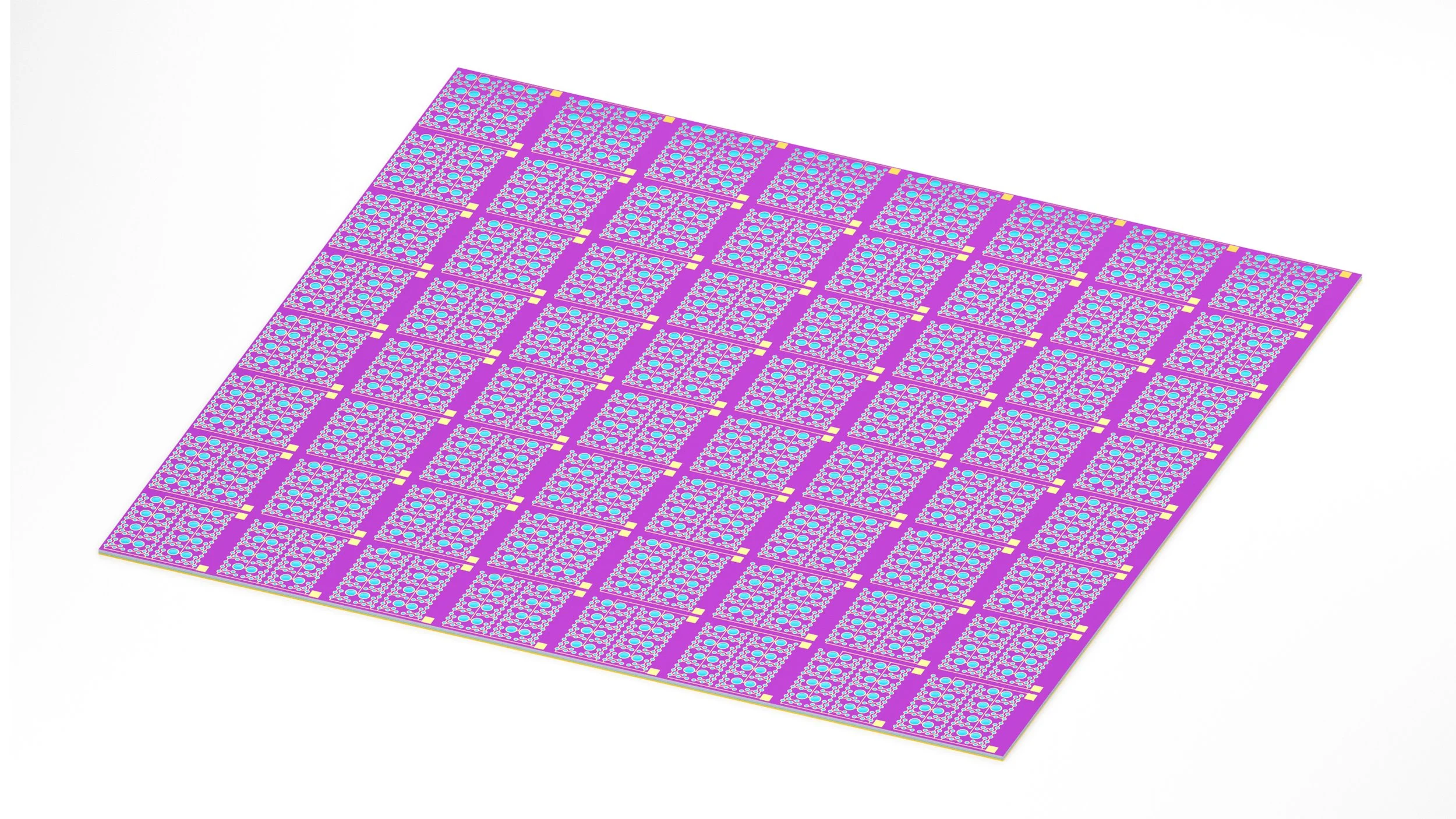
A VCSEL (Vertical-Cavity Surface-Emitting Laser) laser array is a semiconductor chip that integrates many tiny VCSEL emitters on one surface. Each emitter produces a narrow, stable beam, and together they form a dense, controllable light source.
Unlike edge-emitting lasers, a VCSEL laser array emits vertically from the wafer surface. This architecture offers:
Efficient coupling into fibers, waveguides and free-space optics
Low power consumption and high wall-plug efficiency
Excellent wavelength stability over temperature
Simple testing at wafer level, supporting high-volume production
For manufacturers and system integrators, this means scalable optical power, compact footprints and reliable performance in demanding environments.
How Does a VCSEL Laser Array Work?
Inside a VCSEL laser array, each pixel consists of multiple epitaxial layers grown on a GaAs wafer. The active region is sandwiched between distributed Bragg reflector (DBR) mirrors that form a vertical resonant cavity.
When current is injected:
Electrons and holes recombine in the active region.
Photons are generated and amplified within the cavity.
The DBR mirrors confine the light and force it to oscillate at a defined wavelength.
Coherent laser light exits perpendicularly from the top surface.
By arranging many of these emitters into a grid, ring or custom pattern, a VCSEL laser array can deliver:
High optical power density
Uniform illumination for structured light or ToF systems
Fast modulation for data links and high-speed sensing
Ace Photonics optimizes epitaxial design, current confinement and thermal paths so that each array maintains stable output across temperature and long-term operation.
Evolution of VCSEL Technology
VCSEL concepts were explored in the 1970s, and commercial devices began to scale in the 1990s with the rise of short-reach optical communication. Since then, VCSELs have become a core light source in:
Data center interconnects and optical backplanes
3D sensing for smartphones and consumer devices
Automotive and industrial LiDAR
Medical diagnostics and quantum sensing
Modern VCSEL laser arrays benefit from mature GaAs processing, precise wet oxidation and advanced etching techniques, enabling:
Narrow spectral linewidths
High reliability and long lifetimes
Wafer-level binning and cost-effective mass production
Ace Photonics builds on more than 20 years of VCSEL R&D experience, focusing on high-temperature, single-mode and non-magnetic solutions for specialized markets such as quantum applications and industrial automation.
Key Applications of VCSEL Laser Arrays
1. Optical Communication and Data Centers
VCSEL laser arrays are widely used in short-reach and medium-reach optical links:
High-speed data center interconnects
Optical backplanes and active optical cables
5G and edge-computing connectivity
Their benefits include:
Multi-gigabit data rates with low drive currents
Efficient coupling to multimode fibers
Low power consumption and reduced thermal load in racks
By integrating VCSEL arrays with driver ICs and passive optics, data center operators can upgrade bandwidth while controlling power and cooling budgets. Ace Photonics develops VCSEL dies and modules with stable wavelengths for robust, high-density communication links.
2. Sensing, LiDAR and 3D Imaging
VCSEL laser arrays are now central to many sensing and imaging platforms:
Automotive LiDAR and ADAS – Long-range depth sensing, object detection and road profiling
3D facial recognition and access control – Secure, high-resolution depth maps for identity verification
Industrial 3D metrology – Structured-light projection and ToF sensing for inline quality control
In LiDAR and 3D sensing, arrays provide:
Dense dot patterns or tailored illumination geometries
Fast modulation for ToF measurements
Stable IR wavelengths that simplify optical filter design
Ace Photonics designs GaAs-based VCSEL arrays and modules that can be customized for structured light, ToF and active stereo systems, including non-magnetic, high-temperature packaging for harsh environments.
3. Consumer Electronics & Biometrics
Infrared VCSEL laser arrays enable many everyday user experiences:
Face unlock in smartphones and tablets
Gesture recognition in AR/VR headsets
Proximity and presence sensing in wearables and smart home devices
Compared with LEDs, VCSEL arrays offer:
Narrower wavelength spread for more robust algorithms
Higher modulation speeds for secure, anti-spoofing protocols
Uniform illumination across the field of view
Ace Photonics supports compact, low-power VCSEL solutions that integrate easily into mobile, wearable and IoT form factors.
4. Medical and Quantum Technologies
Ace Photonics also supplies VCSEL chips and arrays for specialized markets:
Medical diagnostics and imaging – Stable wavelengths for spectroscopy, pulse oximetry and imaging
Wearable health monitoring – Low-power light sources for continuous SpO₂, glucose and blood pressure tracking
Quantum sensing and atomic devices – Narrow linewidths and specific wavelengths (e.g., 795 nm / 895 nm) used in chip-scale atomic sensors and magnetometers
Custom array layouts, wavelength selection and packaging help device makers meet strict performance and regulatory requirements in healthcare and quantum applications.
Advantages of VCSEL Laser Arrays
From a manufacturer’s perspective, VCSEL laser arrays offer a balanced combination of performance, cost and manufacturability:
High-speed modulation – Supports multi-Gb/s links and fast ToF ranging
Superior beam control – Well-defined beam profiles and pattern shaping for structured light
Energy efficiency – High wall-plug efficiency reduces power and cooling needs
Compact, scalable design – Thousands of emitters on a single chip for high optical density
Wafer-level manufacturing – Facilitates testing, binning and cost-competitive volume production
Temperature and wavelength stability – Often eliminating the need for bulky active temperature control in many systems
Ace Photonics further enhances these advantages with non-magnetic, high-temperature packages and custom epitaxial structures tuned to each application.
Design Challenges and Considerations
Despite their strengths, several design aspects must be managed carefully when integrating VCSEL laser arrays:
Thermal management – Dense emitter layouts can generate significant heat. Substrate choice, heat-spreading design and package materials are critical to maintain junction temperatures and lifetime.
Eye safety and compliance – Especially in consumer and automotive LiDAR applications, system designers must shape and limit optical output to meet laser safety standards.
Optical design – Matching array geometry with microlens arrays, diffusers and system optics determines final beam uniformity and coverage.
Cost vs. performance trade-offs – Higher power or more complex packaging can increase cost; careful optimization is required for high-volume products.
Ace Photonics addresses these challenges through process control, in-line testing and robust packaging strategies designed for industrial-scale deployment.
Market Trends for VCSEL Laser Arrays
The global VCSEL market continues to grow, driven by:
Rising bandwidth demands in data centers
Expansion of LiDAR and 3D sensing in automotive and industry
Increasing use of biometrics and 3D cameras in consumer devices
Adoption of optical and quantum sensing in healthcare and research
Within this market, high-power VCSEL arrays at wavelengths around 795 nm, 895 nm and related bands are gaining attention for industrial, medical and quantum applications.
Manufacturers like Ace Photonics respond by:
Scaling production to reduce cost per watt
Offering more flexible array geometries and custom packaging
Providing engineering support from early design to mass production
Why Choose Ace Photonics for VCSEL Laser Arrays?
Ace Photonics is a dedicated VCSEL manufacturer focused on high-performance, application-specific solutions:
Full product portfolio – VCSEL die, VCSEL packages, VCSEL modules and gain chips to support different integration strategies.
Custom design from wafer to package – Tailored wavelengths, output power, array patterns and packaging for optical communication, LiDAR, 3D sensing, medical and quantum systems.
High-temperature and non-magnetic solutions – Suitable for harsh or magnetically sensitive environments, including aerospace and industrial automation.
Experienced R&D team – A background rooted in the Chinese Academy of Sciences, with long-term expertise in GaAs-based VCSEL processing, ICP etching, wet oxidation and advanced packaging.
From prototype support to volume manufacturing, Ace Photonics works closely with customers to translate system-level requirements into reliable VCSEL laser array solutions that are ready for integration.
Get Started with Custom VCSEL Laser Arrays
Whether you are developing a new LiDAR platform, upgrading data center links or designing a compact sensing module, a well-engineered VCSEL laser array can significantly improve performance and manufacturability.
Contact Ace Photonics to discuss:
Target wavelength and power levels
Required array geometry and beam pattern
Packaging, operating temperature and environmental constraints
Compliance and testing needs for your industry
Our engineering team can help you move from concept to stable, production-ready VCSEL laser array solutions tailored to your application.