
How to Measure Magnetic Cleanliness in VCSEL Packages
Your rubidium vapor cell is stabilized, the optics are aligned, and the driver circuit is tuned. Yet your atomic magnetometer drifts several kilohertz off its target frequency.
You swap out the low-noise amplifier, check the photodiode grounding, and recalibrate the current driver. The drift persists.
The issue is rarely the electronics. Look at the laser package mounted millimeters from the vapor cell. A standard TO-can header contains a sub-micron nickel strike beneath its gold plating. That thin layer turns the component into an uncalibrated permanent magnet, shifting the atomic energy levels you are attempting to measure.
Quantum optics and chip-scale atomic clocks (CSACs) operate on physics where standard optoelectronic packaging fails. Stray magnetic fields from internal packaging materials degrade atomic coherence. Verifying VCSEL magnetic cleanliness requires purpose-built shielding, sensitive magnetometers, and strict material tracking.
The Physics: Why Quantum Sensors Reject Ferromagnetic Packaging
Alkali vapor sensors (principally rubidium-87 and cesium-133) rely on coherent atomic spin states. When an external magnetic field penetrates the vapor cell, energy levels shift via the Zeeman effect:
ΔE = gF μB B mF
Where gF is the Landé g-factor, μB is the Bohr magneton, B is the total magnetic flux density, and mF is the magnetic quantum number.
Atomic magnetometers measure subtle variations in B. If the pump or probe laser package leaks an uncharacterized field into the interaction volume, several problems emerge:
- Systematic Frequency Offsets: The local bias field shifts atomic resonance frequencies away from nominal clock transitions.
- Dephasing and Linewidth Broadening: Inhomogeneous fields across the vapor cell shorten transverse relaxation times (T2), degrading signal-to-noise ratios.
- Thermal and Mechanical Drift: Ferromagnetic domains within the package shift with temperature and mechanical shock, introducing drift that active compensation coils cannot track.
Sources of Magnetic Contamination in Laser Packaging
Contamination originates in standard packaging materials chosen for cost, hermeticity, or thermal expansion matching rather than magnetic neutrality.
| Component | Standard Material | Magnetic Behavior | Quantum-Grade Alternative |
|---|---|---|---|
| Header / Base | Kovar (Fe-Ni-Co) | Ferromagnetic (Br > 0.8 T) | CuW, Phosphor Bronze, Pure Cu |
| Plating Undercoat | Electroless / Electrolytic Nickel | Strongly Ferromagnetic | Titanium, Platinum, or Direct Gold |
| Cap / Can | Deep-drawn Kovar or 304 Stainless | Ferromagnetic via cold work | Non-magnetic brass, copper, ceramic |
| Submount | Metallized AlN (with Ni barrier) | Weak-to-moderate remanence | Ti/Pt/Au metallized AlN or Diamond |
| Window Seal | Ferro-alloy braze or Kovar eyelet | Localized dipole sources | AuSn solder preform, sapphire glass |
Cold-Work Martensite Transformation
Austenitic stainless steels (such as AISI 304) are nominal paramagnets in their annealed state. Stamping, deep drawing, or cutting these metals induces shear strains that transform face-centered cubic (γ) austenite into body-centered tetragonal (α') martensite. A stamped cap that began as non-magnetic stock can exhibit localized remanence exceeding 1 μT after mechanical forming.
Contaminated Plating Baths
Plating baths introduce hidden contamination. Even non-magnetic diffusion barriers, such as copper-phosphorus or pure gold, pick up iron from processing tanks, fixtures, or chemical feedstocks. A bulk material specification alone does not guarantee a magnetically clean finished component.
Building the Measurement Test Bench
Measuring sub-nanotesla fields requires isolating the test environment from background interference. The Earth's magnetic field varies between 30 μT and 60 μT, while electrical lines, building elevators, and passing vehicles produce background noise of hundreds of nanotesla.
- Zero-Field Chamber: Use at least three concentric cylinders of high-permeability mu-metal (μr > 30,000) with nested aluminum layers for dynamic RF attenuation. Residual internal fields must stay below 1 nT.
- De-Gaussing System: Wind an AC de-gaussing coil directly onto the innermost mu-metal layer. Drive it with a decaying low-frequency sine wave (typically 50 Hz to 0.1 Hz) before every measurement shift to purge trapped flux.
- Non-Metallic Fixturing: Ensure every screw, guide rail, and sample holder inside the chamber is constructed from Delrin, PEEK, or virgin PTFE. Brass screws are often contaminated with trace iron and must be screened before installation.
Screening Methods for VCSEL Packages
Two parameters determine packaging cleanliness: Remanent Magnetization (Br, the field emitted with zero external bias) and Magnetic Susceptibility (χ, the field induced when an external field is present).
1. Three-Axis Fluxgate Magnetometry
A miniature fluxgate sensor is the most practical choice for incoming QC and batch screening.
- Setup: Mount the fluxgate probe rigidly at the center of the zero-field shield. Position the packaged VCSEL on a rotary PEEK stage at a fixed standoff distance (r = 3 mm to 10 mm).
- Procedure: Rotate the sample through 360° across two orthogonal axes while recording Bx, By, and Bz.
- Dipole Extraction: An isolated contaminant behaves as a point magnetic dipole. Fitting the sinusoidal modulation from sample rotation isolates the net dipole moment magnitude.
2. Optically Pumped Magnetometers (OPM)
For flight hardware or primary atomic standards requiring fields below 100 pT, fluxgates run into their thermal noise floors (~10 pT/√Hz). Microfabricated rubidium or cesium OPMs achieve sensitivities below 15 fT/√Hz at room temperature, making them well-suited for benchtop sub-nanotesla characterization without cryogenic cooling.
Step-by-Step Package Screening Protocol
Phase 1: Pre-Assembly Inspection
- Inspect Sub-Components: Screen bare headers, submounts, and window caps prior to die bonding. Defective lots should be rejected before adding active epitaxial material.
- Surface Contamination Check: Swipe incoming components across a calibrated high-gradient magnetic field to detect loose machining swarf or plating flakes.
Phase 2: Assembly Control
- Tooling Quarantine: Restrict assembly workstations to non-magnetic tools. Prohibit standard stainless steel tweezers and wire-bonder collets; use grade-5 titanium or ceramic tooling instead.
- Bond Wire Verification: Use high-purity 99.99% gold (4N Au) or aluminum wire. Avoid copper-palladium wires unless their metallurgy is certified free of nickel seeds.
Phase 3: Stress and Stability Verification
- Thermal Cycling: Subject test packages to ten cycles between -40°C and +85°C. Measure the residual dipole moment before and after. Phase transformations in marginal alloys will manifest as increases in remanence.
- Mechanical Shock: Apply a mechanical shock profile to verify that internal bond geometries do not shift or distort relative to the output window.
Customized Non-Magnetic Solutions: Ace Photonics
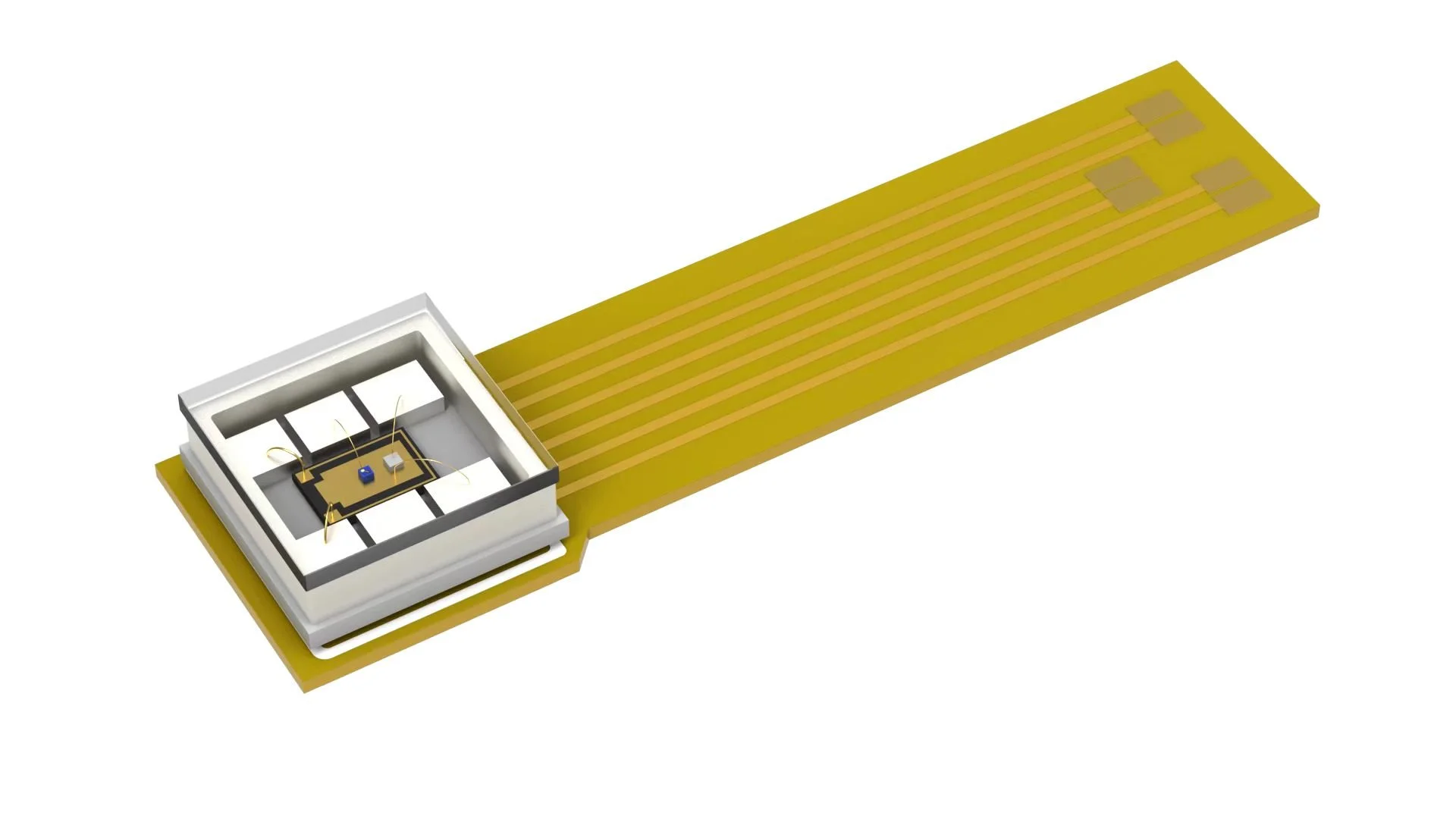
Eliminating parasitic fields requires addressing packaging at the alloy and manufacturing levels. Ace Photonics Co., Ltd. manufactures customized 795nm (Rubidium D1) and 895nm (Cesium D1) single-mode 1mW VCSEL non-magnetic packaging solutions designed specifically for quantum sensing, atomic magnetometry, and atomic clocks.
Standard packaging choices inadvertently ruin sensitive quantum transitions through ferromagnetic hysteresis and bias shifts. Our dedicated process controls ensure non-magnetic integrity from initial submount selection through to hermetic cap sealing.
- Non-Magnetic Architecture: Assemblies replace Kovar and standard nickel barriers with verified copper-tungsten mounts, phosphor bronze pins, and direct-gold finishes.
- Custom Optical Windows: Packaging options include flat or wedged sapphire, anti-reflective coated fused silica, and custom hermetic seals tailored to specific beam geometry and polarizations.
- Screened Manufacturing: Headers, caps, and submounts undergo multi-axis fluxgate testing to verify that residual emissions meet sub-nanotesla criteria.
Common Measurement Pitfalls
- Ignoring Lead Drive Currents: Current passing through laser leads generates a magnetic field. A 2 mA DC bias current running through an unshielded 5 mm trace produces roughly 80 nT at a 5 mm standoff. Use twisted-pair connections or coaxial pins to cancel current-loop areas.
- Imprecise Standoff Control: The magnetic dipole field decays with 1/r3. A positioning error of 0.5 mm at a 3 mm test distance produces an amplitude error of more than 40%. Anchor the test datum against rigid mechanical stops.
- Operator and Environmental Interference: Steel zippers, wristwatch bands, and eyeglass frames within one meter distort picotesla-level readings. Enforce non-magnetic cleanroom apparel for all screening operators.
Frequently Asked Questions
What magnetic cleanliness limit is standard for quantum sensors?
Most chip-scale atomic clocks and vapor-cell magnetometers set a limit of less than 1 nT residual field at a distance of 5 mm to 10 mm. High-performance atomic gyroscopes often tighten this limit to less than 100 pT.
Can de-gaussing make a standard Kovar package usable?
No. De-gaussing removes remanent magnetization, but Kovar maintains high magnetic susceptibility (μr ≈ 100–1,000). Any ambient field will induce immediate magnetization in the Kovar base, distorting the local field.
Why use VCSELs rather than edge-emitting DFB lasers in atomic sensors?
VCSELs consume milliwatts of electrical power compared to hundreds of milliwatts for DFBs, provide circular, low-divergence output beams, and emit normal to the surface, making them well-suited for compact, low-power non-magnetic packaging.
Does the window material influence package magnetism?
Pure fused silica and sapphire are diamagnetic and do not generate parasitic fields. However, metal coatings on window edges, metallized solder preforms, and braze alloys used for hermetic sealing can introduce ferromagnets if not specified as non-magnetic grades.
How do you separate remanent field from induced field during testing?
Measure the package twice inside the shielded chamber. First, test with all internal compensation coils off (Bext ≈ 0) to measure remanent magnetization. Next, apply a known, uniform bias field (such as 50 μT) using Helmholtz coils. Subtracting the baseline applied field from the reading isolates the induced magnetization.