

VCSEL Package Options for Quantum Sensing, 3D Sensing, and OEM Applications
When evaluating a VCSEL device, many buyers look at the chip first. That is important, but in actual use, the vcsel package also has a big influence on performance. It affects thermal behavior, optical stability, reliability, and how easily the device can be integrated into the final system.
For applications such as quantum sensing, 3D sensing, gas sensing, and custom OEM projects, packaging is not just an outer shell. It is part of the solution. Different systems need different structures, materials, and integration methods, which is why Ace Photonics offers VCSEL die, packaged devices, modules, and custom OEM support for demanding photonics applications.
What a VCSEL Package Actually Does
A vcsel package is not only there to protect the chip. It also helps with electrical connection, heat dissipation, mechanical stability, and in some cases optical alignment.
In practice, the right package depends on what the laser is being used for. A compact consumer product may need a small SMD structure that works well with PCB assembly. A precision sensing system may care more about non-magnetic materials. An OEM project may need a custom housing with a lens, window, or temperature control design.
Common VCSEL Package Types
Instead of describing each package type in long blocks of text, it is often clearer to compare them side by side.
This kind of layout makes the information easier to scan and feels more like a real technical buying guide than a generic article.
TO-Can VCSEL Package
The TO-can remains one of the most familiar vcsel package formats. Many customers still choose it because it is practical, proven, and relatively easy to integrate into existing systems.
For standard industrial and research projects, TO-can packaging is often a safe choice. It works well in many conventional optical and electrical setups. But it also has limits. Ace Photonics notes that some traditional TO-46 packages may include magnetic components, which can create problems in ultra-sensitive systems such as atomic magnetometers. In that kind of application, the package material is no longer a small detail. It becomes part of the measurement challenge.


SMD VCSEL Package
If compact integration and manufacturing efficiency are the main priorities, an smd vcsel package is usually the better fit.
SMD packaging is easier to use in products built around PCB assembly and SMT processes. It is especially suitable for smaller electronic systems where board space is limited and the design has to scale into volume production. That is why SMD VCSELs are often associated with 3D sensing, wearable electronics, proximity sensing, AR/VR, and health monitoring devices.
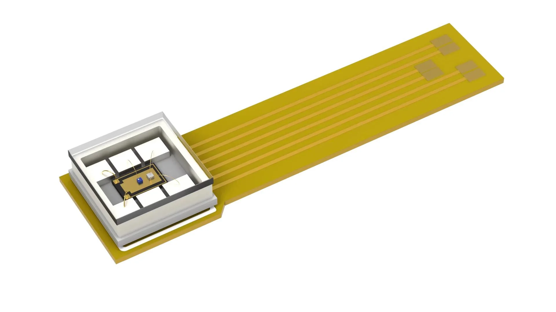
Ceramic and Custom VCSEL Package Designs
Standard package formats are not enough for every project. In many photonics systems, performance depends on more than just the chip and wavelength. The housing, thermal path, optical window, and assembly structure can all influence the final result.
Ace Photonics states that it supports packaging from concept to mass production and can customize package types including TO-can, SMD, ceramic, and other custom housings. For OEM customers, that flexibility matters because real-world system requirements are often much more specific than a standard catalog format can handle.
A custom vcsel package may include non-magnetic materials, TEC structures, temperature sensors, beam shaping, lens design, windows, PCBs, drivers, or module-level integration. That makes custom packaging a better option when the application has strict demands on optics, thermal control, or system assembly.

Why Non-Magnetic VCSEL Package Design Matters
One useful point in your original content is the emphasis on non-magnetic vcsel package design. This makes the article feel more specific and less like a general packaging overview.
In applications such as atomic magnetometers, quantum gyroscopes, atomic clocks, MRI-related systems, and other precision sensing environments, small magnetic interference can affect measurement quality. In these cases, packaging is not just about size, cost, or convenience. It directly affects whether the system can perform as intended.
Which VCSEL Package Fits Which Application
This section is also a good place to use a table. It breaks up the page nicely and makes the article feel less generated.
Compared with plain paragraphs, this kind of table feels more practical and easier for readers to use. It also makes the page look more like a commercial or engineering reference article.
What Customers Should Look for in a VCSEL Package Supplier
The package itself matters, but supplier capability matters too. Customers usually do not just need a housing. They need a supplier that can connect chip design, thermal management, package structure, and application requirements into one workable product.
Ace Photonics highlights long-term VCSEL R&D experience, GaAs-based VCSEL development, custom epitaxial and device structure design, non-magnetic packaging, high-temperature VCSEL solutions up to 150°C, and customization from wafer to package level. For OEM customers, this kind of support can help shorten development time and reduce design revisions during the project cycle.
Conclusion
There is no single vcsel package that works best for every application.
For compact electronics, SMD is often the practical choice. For standard industrial or research use, TO-can is still widely accepted. For applications with stricter thermal, optical, or structural demands, ceramic and custom packages offer more room for engineering optimization. And for quantum sensing or other ultra-sensitive systems, a non-magnetic package may be essential rather than optional.
That is also where Ace Photonics has a clearer position in the market: not just supplying VCSEL chips, but supporting customers with package, module, and OEM development options built around real application needs.