
Purpose-Built for Quantum technology
We develop precision VCSEL solutions for atomic clocks, quantum technology,
and advanced photonic systems for research, industrial, and emerging quantum applications.
VCSEL Reliability and Lifetime Prediction: A Practical Guide to HTOL and FIT Rate Testing
A test engineer once told me that vertical-cavity lasers don't die of natural causes—they are murdered by heat and current crowding. He wasn't wrong.
You run an optical transceiver, atomic clock, or automotive lidar array. The drive board feeds clean current, but the emitter goes dark. Pull the component, put it under a bench microscope, and the aperture looks untouched. No charred facet. No smoke.
GaAs physics simply collected its debt.
Every optoelectronics catalog claims an operating lifetime of "over 100,000 hours." Those numbers are paper promises unless backed by actual accelerated stress runs. Evaluating true laser longevity requires looking past vendor marketing, picking apart VCSEL reliability physics, stress-testing under High-Temperature Operating Life (HTOL testing VCSEL) racks, and deriving honest Failures in Time (FIT) metrics.
1. The Mechanics of Laser Cavity Failure
Edge-emitting laser diodes suffer from Catastrophic Optical Mirror Damage (COMD). Their mirrors sit exposed to ambient air; intense photon densities at the output facet trigger localized melting.
VCSELs sidestep that problem because light leaves vertically through distributed Bragg reflector (DBR) stacks embedded inside the semiconductor lattice. Yet they swap one failure mode for an equally unforgiving thermal bottleneck.
Dark Line Defects: The Internal Parasite
Dark Line Defects (DLDs) represent the primary killer in Vertical-Cavity Surface-Emitting Lasers. A DLD begins as an imperceptible crystal dislocation or shear stress point left behind during wafer epitaxial growth, contact metallization, or die singulation.
Turn the drive current on, and non-radiative carrier recombination takes over. Instead of shedding clean photons, that dislocation site captures injected electrons and converts their energy straight into localized heat.
The dislocation climbs. It threads through the gallium arsenide quantum wells, growing a microscopic network of non-radiative paths. Under photoluminescence inspection, you see dark, web-like bands spreading across the optical emission zone. Once a DLD spans the emission aperture:
Threshold current spikes upward.
Slope efficiency collapses.
The optical output flatlines.
Aperture Stress and Current Crowding
To force photons into a tight, circular beam, wafer fabs use selective lateral wet oxidation. Aluminum-rich layers within the epitaxial structure oxidize into insulating material, creating a tiny central aperture—often 4 to 10 microns across.
This oxidation alters the local lattice volume, locking mechanical strain directly at the oxidation tip. When current flows, it crowds along this exact boundary. You get an intense local thermal peak right where mechanical stress is highest. Any minor flaw in oxidation temperature or vapor control leaves a built-in point of failure.
2. Accelerated Stress Testing: HTOL Protocols
Waiting twenty years to observe natural device degradation is obviously impossible for product development cycles. High-Temperature Operating Life (HTOL) testing accelerates normal operating degradation into manageable laboratory schedules.
Setting the HTOL Parameters
During HTOL, dozens or hundreds of devices sit in specialized burn-in boards inside high-temperature ovens. They run under continuous wave (CW) forward bias.
High-stress ovens age dies rapidly. Periodic in-situ or benchtop characterization tracks three baseline metrics:
L-I-V Curves: Shifts in threshold current, maximum optical rollover power, and forward operating voltage.
Reverse Leakage Current: Spikes in reverse leakage current point toward dielectric breakdown or junction contamination.
Spectral Stability: Center wavelength shift and side-mode suppression ratio (SMSR) drift under temperature.
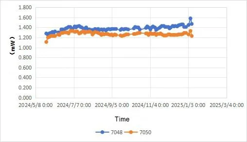
A device fails when its optical output power drops by more than 20% (or 1.0 dB to 1.5 dB, depending on system requirements) at standard room-temperature bias, or if threshold current jumps beyond specified thresholds.
Industry Qualification Standards
Laser reliability standards depend on deployment environments:
Telcordia GR-468-CORE: The benchmark for telecommunications and datacom equipment. Requires minimum 2,000-hour HTOL testing across separate wafer lots without random infant failures.
MIL-STD-883: Dictates environmental, mechanical, and thermal endurance (Method 1005 for steady-state life) in defense, aerospace, and harsh operational setups.
AEC-Q102: Automotive standard requiring rigorous operating life testing alongside rapid thermal cycling from -40°C to +125°C.
3. Deriving FIT Rates from HTOL Datasets
Turning thousands of oven hours into a single actionable reliability number requires empirical physics and statistical estimation.
The Acceleration Factor (AF)
Total acceleration links thermal stress and electrical current density using an Arrhenius-Eyring relationship:
4. Burn-In Strategies: Wafer-Level vs. Package-Level
Burn-in filters out infant mortality before lasers reach end-use circuit boards. The manufacturing dilemma centers on timing: weed out bad chips on the uncut wafer, or package them first?
When comparing wafer-level burn-in vs package-level burn-in for VCSEL dies, volume economics drive the decision.
Consumer 3D sensing arrays often justify expensive wafer-level probing to protect packaging yields. High-reliability telecom transceivers, medical sensors, and military systems still rely on package-level screening. Probing a bare wafer cannot reveal assembly defects, such as voids in the submount solder interface or micro-cracks from wire-bonding.
5. Precision Packaging: The Non-Magnetic Frontier
While datacom hardware tolerates standard nickel-plated Kovar headers, high-sensitivity quantum applications operate under completely different rules.
Miniaturized quantum sensors—such as Chip-Scale Atomic Clocks (CSAC) and optically pumped rubidium magnetometers—rely on ultra-stable atomic transitions. Driving these systems requires narrow-linewidth optical pumping, precisely targeted at:
Ferromagnetic materials create parasitic magnetic fields. Placing a standard nickel-plated laser diode adjacent to an alkali vapor cell causes stray magnetic fields that induce unwanted Zeeman splitting in the vapor's atomic energy levels.
This Zeeman shift pulls the absorption frequency off center, degrading clock timing and lowering sensor sensitivity.
To address this challenge, Ace Photonics Co., Ltd. manufactures tailored 795nm and 895nm 1mW VCSEL non-magnetic packaging solutions designed for field-grade quantum sensors.
Our assembly flow replaces standard ferrous iron-nickel alloys with precision-machined titanium, gold-plated copper-tungsten mounts, and non-magnetic aluminum sub-mounts. This completely eliminates residual magnetic signatures.
To maintain spectral performance, we customize window profiles to client optical requirements:
Hermetically sealed flat sapphire windows.
Tilted AR-coated glass (defeating optical feedback that degrades linewidth).
Wedge optics matched directly to target rubidium or cesium cells.
Surface-mount (SMD) or classic transistor-outline (TO) footprints.
6. Long-Term Reliability Best Practices
Keeping vertical-cavity lasers alive over decades comes down to practical operating safeguards:
Control Electrostatic Discharge (ESD): A human body discharges thousands of static volts without noticeable sensation. A reverse spike as low as 50V can punch through an aperture's thin oxide layer, sparking immediate crystal damage. Use grounded benches, dissipative carriers, and local transient voltage suppression (TVS) diodes.
Respect the Thermal Path: Gallium arsenide conducts heat poorly compared to silicon. Run thermal simulations on die-attach solder bonds to minimize voids. Every 10°C drop in operating junction temperature roughly doubles the emitter's operational life.
Suppress Inductive Drive Ringing: VCSELs respond quickly to nanosecond modulation signals. Poorly matched board traces or long leads introduce parasitic inductance, causing forward current overshoot that stresses the aperture edge. Tune drive networks with snubber circuits to suppress turn-on ringing.
Frequently Asked Questions (FAQs)
What is the typical difference between infant mortality and wear-out failures in a VCSEL?
Infant mortality happens within the first 24 to 500 operating hours. It stems from manufacturing flaws like epilayer defects, oxide strain, or micro-cracks caused by wafer saw dicing. Wear-out represents the gradual, long-term degradation of the crystal lattice—such as slow dopant migration or point defect accumulation—typically observed after tens of thousands of continuous operational hours.
Why does calculating FIT rate require junction temperature rather than ambient temperature?
DBR mirror stacks exhibit high thermal impedance, often exceeding 1000 K/W. Because current funnels through a tiny aperture, internal junction temperatures run 15°C to 50°C higher than ambient air or heat sink temperatures. Calculating the thermal acceleration factor with ambient temperature underestimates physical cavity stress, yielding dangerously optimistic reliability projections.
How do I choose the correct activation energy value for reliability models?
Empirical testing across two or more elevated junction temperatures provides the actual Arrhenius slope for a specific fab process. When empirical test data is unavailable, industry standards for GaAs/AlGaAs devices typically use values between 0.65 eV and 0.75 eV. Using values near or above 1.0 eV without empirical justification artificially suppresses calculated FIT rates.
Why is optical feedback particularly damaging to single-mode VCSEL reliability?
Reflected photons re-entering the laser cavity cause coherent optical interference, inducing mode hopping, intensity noise, and threshold instability. In high-power scenarios, severe back-reflections can cause localized optical field spikes inside the quantum well layers, accelerating thermal degradation near the aperture.
Can non-magnetic packaging be customized for high-temperature atomic sensors?
Yes. Packaging for atomic vapor sensors can incorporate high-temperature brazing alloys alongside zero-ferrous materials like copper-tungsten and titanium. These assemblies remain mechanically and hermetically stable at temperatures above 85°C to 100°C without generating stray magnetic fields that interfere with vapor cell resonance.